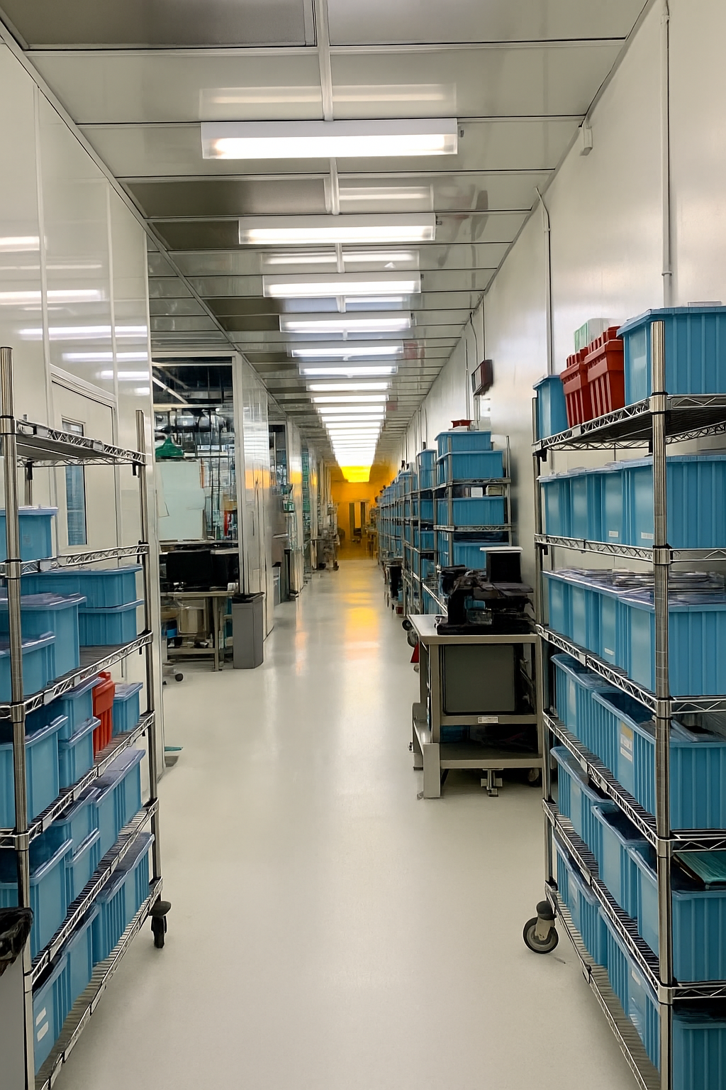
Cleanroom Capabilities
Vacuum deposition:
Sputtering with in-situ ion-milling. Dedicated chambers to superconductors, magnetic materials, and dielectrics
Ebeam evaporation dedicated to metals (lift-off and conformal deposition) and dielectrics. In-situ ion-milling available
ALD dedicated to metals and high-K dielectrics
Thermal evaporation
PECVD
ICP-PECVD
MVD

Etching:
ICP, RIE, IBE
Fluorine etcher
Atomic layer etching (ALE)
Deep Si etcher
Plasma cleaning and activation
Asher
Focused ion beam lithography
Lithography:
MLA laser writer (500 nm resolution)
Stepper and ASML lithography (500 and 200 nm resolution)
Ebeam lithography (Raith)
Focused ion beam lithography (Raith)
Mask aligner (MJB-3 and SUSS MA-6)
Wet processing:
Solvent
Developing
Plating
Corrosive
HF
Polishers
Thermal processing:
Various furnaces, ovens, and RTAs
Packaging:
Automated dicing
Automated cleaver
Flip-chip bonder
Wafer bonder
Wafer/wax bonder
Wire bonder
PCB
Soldering
Material characterization:
SEM/EDAX
FIB/STEM
AFM
XRD
Profilometers
Ellipsometer
Optical film thickness & wafer mapping
DUV optical microscope
Laser scanning confocal microscope
Film stress
Particle count
Device Characterization Capabilities
Electrical characterization:
Probe station
CV and IV measurements
High frequency measurements
Cryogenic (PPMS 1.8-400 K) electrical low noise, heat capacity, and magnetotransport/Hall measurements
Optical characterization:
Pulsed Pump-probe spectrocopy
EQE measurements
PL measurements